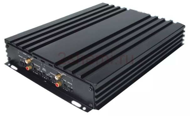
Scheme No. 1
Amplifier class selection . We will immediately warn the radio amateur - we will not make a class A amplifier on transistors. The reason is simple - as mentioned in the introduction, the transistor amplifies not only the useful signal, but also the bias applied to it. In other words, it amplifies direct current. This current, together with the useful signal, will flow through acoustic system(AC), and the speakers, unfortunately, are able to reproduce this direct current. They do this in the most obvious way - pushing or pulling the diffuser from the normal position to the unnatural.
Try to press the speaker cone with your finger - and you will see what a nightmare this sound will turn into. Direct current in its action successfully replaces your fingers, so it is absolutely contraindicated for a dynamic head. To separate the direct current from the alternating signal is possible only by two means - a transformer or a capacitor - and both options, as they say, one is worse than the other.
The diagram of the first amplifier that we will assemble is shown in fig. 11.18.
This is a feedback amplifier whose output stage operates in mode B. The only advantage of this circuit is its simplicity, as well as the uniformity of the output transistors (no special complementary pairs are required). However, it is widely used in low power amplifiers. Another plus of the scheme is that it does not require any configuration, and with serviceable parts it will work right away, and this is very important for us now.
Let's take a look at how this circuit works. The amplified signal is fed to the base of the transistor VT1. The signal amplified by this transistor from the resistor R4 is fed to the base of the composite transistor VT2, VT4, and from it to the resistor R5.
Transistor VT3 is turned on in emitter follower mode. It amplifies the positive half-waves of the signal on the resistor R5 and feeds them through the capacitor C4 to the AC.
The negative half-waves are enhanced by the composite transistor VT2, VT4. In this case, the voltage drop across the diode VD1 closes the transistor VT3. The signal from the output of the amplifier is fed to the circuit divider feedback R3, R6, and from it - to the emitter of the input transistor VT1. Thus, the transistor VT1 plays the role of a comparison device in the feedback circuit.
It amplifies the direct current with a gain equal to unity (because the resistance of the capacitor C direct current theoretically infinite), and the useful signal - with a coefficient equal to the ratio R6 / R3.
As you can see, the value of the capacitance of the capacitor in this formula is not taken into account. The frequency starting from which the capacitor can be neglected in the calculations is called the cutoff frequency of the RC chain. This frequency can be calculated using the formula
F = 1 / (R×C).
For our example, it will be about 18 Hz, i.e. more low frequencies the amplifier will amplify worse than it could.
Pay . The amplifier is assembled on a board made of one-sided fiberglass with a thickness of 1.5 mm and dimensions of 45 × 32.5 mm. PCB layout in mirror image and parts layout can be downloaded. Video of the amplifier in operation MOV format you can download to view. I want to immediately warn the radio amateur - the sound reproduced by the amplifier was recorded in the video using the microphone built into the camera, so speaking about the sound quality, unfortunately, would not be entirely appropriate! Appearance amplifier is shown in fig. 11.19.
Element base . In the manufacture of the amplifier, transistors VT3, VT4 can be replaced by any ones designed for a voltage of at least the supply voltage of the amplifier, and admissible current not less than 2 A. Diode VD1 must be designed for the same current.
The rest of the transistors are any allowable voltage not less than the supply voltage, and the permissible current is not less than 100 mA. Resistors - any with a permissible power dissipation of at least 0.125 W, capacitors - electrolytic, with a capacity not less than indicated on the diagram, and an operating voltage less than the amplifier supply voltage.
Amplifier Heatsinks . Before trying to make our second design, let's, dear radio amateur, dwell on the radiators for the amplifier and give here a very simplified method for calculating them.
First, we calculate the maximum power of the amplifier using the formula:
P = (U × U) / (8 × R), W,
where U- amplifier supply voltage, V; R- AC resistance (usually it is 4 or 8 ohms, although there are exceptions).
Secondly, we calculate the power dissipated on the collectors of transistors, according to the formula:
P race = 0.25 × P, W.
Thirdly, we calculate the radiator area required to remove the corresponding amount of heat:
S \u003d 20 × P races, cm 2
Fourthly, we select or manufacture a radiator, the surface area of \u200b\u200bwhich will be at least calculated.
This calculation is very approximate, but for amateur radio practice it is usually sufficient. For our amplifier, with a supply voltage of 12 V and an AC resistance of 8 ohms, the “correct” radiator would be an aluminum plate measuring 2 × 3 cm and at least 5 mm thick for each transistor. Keep in mind that a thinner plate does not transfer heat well from the transistor to the edges of the plate. I would like to immediately warn you - the radiators in all other amplifiers must also be of “normal” size. Which ones - count for yourself!
Sound quality . After assembling the circuit, you will find that the sound of the amplifier is not entirely clear.
The reason for this is the “pure” class B mode in the output stage, the characteristic distortions of which even the feedback cannot fully compensate for. For the sake of experiment, try replacing the VT1 transistor in the circuit with the KT3102EM, and the VT2 transistor with the KT3107L. These transistors have a much higher gain than KT315B and KT361B. And you will find that the sound of the amplifier has improved significantly, although some distortion will still be noticeable.
The reason for this is also obvious - a larger gain of the amplifier as a whole provides greater accuracy of the feedback, and its greater compensating effect.
Continue reading
The power supply must provide a stable or unstable bipolar supply voltage of ±45V and a current of 5A. This ULF transistor circuit is very simple, since a pair of powerful complementary Darlington transistors is used in the output stage. In accordance with the reference characteristics, these transistors can switch current up to 5A at an emitter-collector junction voltage of up to 100V.
The ULF scheme is shown in the figure below.
The signal requiring amplification through the preliminary ULF is fed to the preliminary differential amplifying stage built on composite transistors VT1 and VT2. The use of a differential circuit in the amplifying stage reduces noise effects and provides negative feedback. The OS voltage is supplied to the base of the transistor VT2 from the output of the power amplifier. DC OS is implemented through resistor R6. The OS for the variable component is carried out through the resistor R6, but its value depends on the ratings of the R7-C3 chain. But it should be borne in mind that too much increase in the resistance R7 leads to excitation.

The DC operation mode is provided by the selection of resistor R6. The output stage on Darlington transistors VT3 and VT4 operates in class AB. Diodes VD1 and VD2 are needed to stabilize the operating point of the output stage.
Transistor VT5 is designed to build up the output stage, its base receives a signal from the output of a differential preamplifier, as well as a constant bias voltage, which determines the mode of operation of the output stage for direct current.
All circuit capacitors must be rated for a maximum DC voltage of at least 100V. It is recommended to mount the output stage transistors on radiators with an area of at least 200 cm squared.
The considered circuit of a simple two-stage amplifier is designed to work with headphones or for use in simple devices with preamp function.
The first transistor of the amplifier is connected according to the circuit with a common emitter, and the second transistor with a common collector. The first stage is designed for basic signal amplification by voltage, and the second stage is already amplifying by power.

The low output impedance of the second stage of a two-stage amplifier, called an emitter follower, allows you to connect not only high-impedance headphones, but also other types of acoustic signal converters.
This is also a two-stage ULF circuit made on two transistors, but already of opposite conductivity. Her main feature that the connection between the cascades is direct. Covered by the OOS through the resistance R3, the bias voltage from the second stage passes to the base of the first transistor.

Capacitor C3, shunts resistor R4, reduces OOS for alternating current, thereby reducing the gain of VT2. By selecting the value of the resistor R3, the operation mode of the transistors is set.
UMZCH on two transistors |

This fairly lightweight power amplifier audio frequency(UMZCH) can be soldered on just two transistors. With a supply voltage of 42V DC, the output power of the amplifier reaches 0.25 W at a load of 4 ohms. Current consumption is only 23 mA. The amplifier operates in single-cycle mode "A".
The low frequency voltage from the signal source is suitable for the volume control R1. Further, through a protective resistor R3 and a capacitor C1, the signal is based on a bipolar transistor VT1 connected according to a common emitter circuit. The amplified signal is fed through R8 to the gate of a powerful field effect transistor VT2 connected according to the scheme with a common source and its load serves primary winding step-down transformer A dynamic head or speaker system can be connected to the secondary winding of the transformer.
In both transistor cascades, there is local negative feedback for direct and alternating current, as well as for the common OOS circuit.
In the case of an increase in the voltage at the gate of a field-effect transistor, the drain-source resistance of its channel decreases and the voltage at its drain decreases. This also affects the signal level supplied to the bipolar transistor, which reduces the gate-source voltage.
Together with the local negative feedback circuits, the operating modes of both transistors are thus stabilized even in the case of a slight change in the supply voltage. The gain depends on the ratio of the resistances of the resistors R10 and R7. Zener diode VD1 is designed to prevent the failure of the field effect transistor. The amplifier stage on VT1 is powered through an RC filter R12C4. Capacitor C5 is a blocking capacitor in the power circuit.
The amplifier can be assembled printed circuit board dimensions 80 × 50 mm, it contains all the elements except for a step-down transformer and a dynamic head

Adjustment of the amplifier circuit is carried out at the supply voltage at which it will operate. For fine tuning it is recommended to use an oscilloscope, the probe of which is connected to the drain terminal of the field-effect transistor. By applying a sinusoidal signal with a frequency of 100 ... 4000 Hz to the input of the amplifier, by adjusting the tuning resistor R5, they ensure that there are no noticeable distortions of the sinusoid with the largest possible amplitude of the signal amplitude at the drain output of the transistor.
The output power of the field-effect transistor amplifier is small, only 0.25W, the supply voltage is from 42V to 60V. Dynamic head impedance 4 Ohm.
Audio signal through variable resistance R1, then R3 and separating capacitance C1 enters the amplifying stage on a bipolar transistor according to a common emitter circuit. Coming from this transistor amplified signal through the resistance R10 passes to the field effect transistor.

The primary winding of the transformer is the load for the field-effect transistor, and a four-ohm dynamic head is connected to the secondary winding. The ratio of the resistances R10 and R7 sets the degree of voltage gain. In order to protect the unipolar transistor, a zener diode VD1 is added to the circuit.
All denominations of parts are on the diagram. The transformer can be used like TVK110LM or TVK110L2, from a frame scanner of an old TV or similar.
UMZCH according to the Ageev scheme |
I stumbled upon this circuit in an old issue of the radio magazine, the impressions from it remained the most pleasant, firstly, the circuit is so simple that even a novice radio amateur can assemble it, and secondly, provided that the components are working and the setup is properly assembled, it does not require.

If you are interested in this circuit, then you can find the rest of the details on its assembly in the radio magazine No. 8 for 1982.
High quality transistorized ULF |
There was a desire to collect more powerful amplifier"A" class. Having read a sufficient amount of relevant literature and chose the most latest version. It was a 30W amplifier that matched high-end amplifiers in terms of its parameters.
I did not intend to make any changes to the existing trace of the original printed circuit boards, however, due to the lack of original power transistors, a more reliable output stage was chosen using 2SA1943 and 2SC5200 transistors. The use of these transistors eventually made it possible to provide a large output power of the amplifier. Schematic diagram of my version of the amplifier below.

This is an image of boards assembled according to this scheme with Toshiba 2SA1943 and 2SC5200 transistors.

If you look closely, you can see on the printed circuit board, along with all the components, there are bias resistors, they are 1 W carbon type. It turned out that they are more thermally stable. During operation of any high power amplifier, huge amount heat, so maintaining the constancy of the nominal electronic component when it is heated is an important condition for the high-quality operation of the device.

The assembled version of the amplifier operates at a current of about 1.6 A and a voltage of 35 V. As a result, 60 watts of continuous power is dissipated in the transistors in the output stage. I must say that this is only a third of the power that they are able to withstand. Try to imagine how much heat is released on the radiators when they are heated to 40 degrees.

The body of the amplifier is handmade from aluminum. Top plate and mounting plate 3 mm thick. The radiator consists of two parts, its overall dimensions are 420 x 180 x 35 mm. Fasteners - screws, mostly with stainless steel countersunk head and M5 or M3 thread. The number of capacitors has been increased to six, their total capacity is 220,000 microfarads. A 500 W toroidal transformer was used for power supply.

Amplifier power supply
The amplifier device is clearly visible, which has copper tires of the appropriate design. A small toroid has been added to regulate the supply under the control of the DC protection circuit. There is also an RF filter in the power circuit. For all its simplicity, I must say deceptive simplicity, the topology of the board of this amplifier and the sound is produced by it, as it were, without any effort, which in turn implies the possibility of its infinite amplification.
Oscillograms of the amplifier
Roll-off 3 dB at 208 kHz

Sine wave 10 Hz and 100 Hz

Sine wave 1 kHz and 10 kHz
100 kHz and 1 MHz signals

Square wave 10 Hz and 100 Hz

Square wave 1 kHz and 10 kHz

Total power 60 W, symmetry cutoff at 1 kHz


Thus, it becomes clear that a simple and high-quality UMZCH design is not necessarily done using integrated circuits - only 8 transistors make it possible to achieve decent sound with a circuit that can be assembled in half a day.
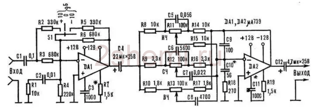
Recently, a certain person turned to him with a request to assemble an amplifier of sufficient power and separate amplification channels for low, medium and high frequencies. before that, I had already collected it for myself more than once as an experiment, and, I must say, the experiments were very successful. The sound quality of even inexpensive speakers is not very good. high level in this case, it improves noticeably in comparison, for example, with the option of using passive filters in the columns themselves. In addition, it becomes possible to quite easily change the crossover frequencies and the gain of each individual band and, thus, it is easier to achieve a uniform frequency response of the entire sound amplifying path. In the amplifier, ready-made circuits were used, which had previously been tested more than once in simpler designs.
Structural scheme
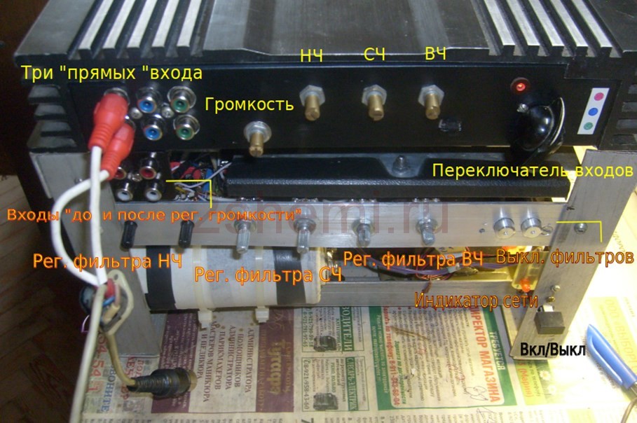
The figure below shows the diagram of 1 channel:

As you can see from the diagram, the amplifier has three inputs, one of which provides for a simple possibility of adding a preamplifier-corrector for a vinyl player (if necessary), an input switch, a preamplifier-timbral lock (also three-band, with adjustable HF / MF / LF levels), volume control, filter unit for three bands with adjustable gain level for each band with the ability to turn off filtering, and a power supply for high-power final amplifiers (unstabilized) and a stabilizer for the “low-voltage” part (preliminary amplification stages).
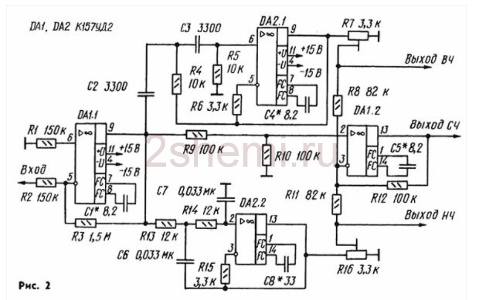
Pre-amplifier tone block
A scheme was used as it, which had been tested more than once before, which, with its simplicity and availability of details, shows quite good performance. The scheme (like all subsequent ones) was once published in the Radio magazine and then published more than once on various sites on the Internet:
The input stage on DA1 contains a gain level switch (-10; 0; +10 dB), which simplifies the coordination of the entire amplifier with signal sources of different levels, and the tone control is directly assembled on DA2. The circuit is not capricious to some variation in the values of the elements and does not require any adjustment. As an op-amp, you can use any microcircuits used in audio paths amplifiers, for example here (and in subsequent circuits) I tried imported BA4558, TL072 and LM2904. Any one will do, but it is better, of course, to choose op-amp options with the lowest possible level of intrinsic noise and high speed (input voltage rise ratio). These parameters can be found in reference books (datasheets). Of course, it is not at all necessary to use this particular scheme here; it is quite possible, for example, to make not a three-band, but a regular (standard) two-band timbre block. But not a "passive" circuit, but with amplification-matching stages at the input and output on transistors or op-amps.
Filter block
Filter circuits, also, if desired, you can find a lot, since there are enough publications on the topic of multiband amplifiers now. To facilitate this task and just as an example, I will give here a few possible schemes found in various sources:
- the circuit that was used by me in this amplifier, since the crossover frequencies turned out to be just the ones that the “customer” needed - 500 Hz and 5 kHz, and nothing had to be recalculated.
- the second scheme, simpler on the OS.
And another possible circuit, on transistors:
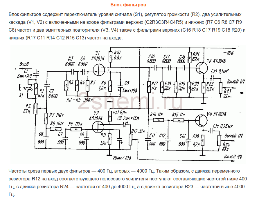
As yours already wrote, I chose the first scheme because of the rather high-quality band filtering and the compliance of the band separation frequencies with the given ones. Only at the outputs of each channel (band) were added simple gain level controls (as is done, for example, in the third circuit, on transistors). Regulators can be set from 30 to 100 kOhm. Operational amplifiers and transistors in all circuits can be replaced with modern imported ones (taking into account the pinout!) To obtain better circuit parameters. All these schemes do not require any adjustment, if it is not required to change the crossover frequencies. Unfortunately, I don’t have the opportunity to give information on the recalculation of these section frequencies, since the circuits were searched for “ready-made” examples and detailed descriptions were not attached to them.
In the filter block circuit (the first circuit of three), the ability to disable filtering for the midrange and high-frequency channels was added. For this, two push-button switches of the P2K type were installed, with which you can simply close the connection points of the filter inputs - R10C9 with their corresponding outputs - “high-frequency output” and “mid-range output”. In this case, the full sound signal goes through these channels.
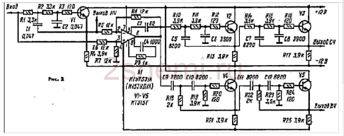
Power Amplifiers
From the output of each filter channel, the HF-MF-LF signals are fed to the inputs of power amplifiers, which can also be assembled according to any of the known schemes, depending on the required power of the entire amplifier. I made UMZCH according to the scheme known for a long time from the Radio magazine, No. 3, 1991, p.51. Here I give a link to the "original source", since there are many opinions and disputes about this scheme about its "quality". The fact is that at first glance this is a class “B” amplifier circuit with the inevitable presence of “step” type distortions, but this is not so. The circuit uses current control of the output stage transistors, which allows you to get rid of these shortcomings with the usual, standard inclusion. At the same time, the circuit is very simple, not critical to the parts used, and even transistors do not require special preliminary selection in terms of parameters. In addition, the circuit is convenient in that powerful output transistors can be placed on one heat sink in pairs without insulating gaskets, since the collector leads are connected at the point " output", which greatly simplifies the installation of the amplifier:

When setting up, it is only IMPORTANT to choose the correct operating modes for the transistors of the final stage (by selecting resistors R7R8) - on the bases of these transistors in the “rest” mode and without load, the output (speaker) should have a voltage within 0.4-0.6 volts. The supply voltage for such amplifiers (there should be 6 of them, respectively) was raised to 32 volts with the replacement of the output transistors with 2SA1943 and 2SC5200, the resistance of the resistors R10R12 should also be increased to 1.5 kOhm (to "make life easier" for the zener diodes in the circuit power input op amps). The op amps were also replaced by the BA4558, and the “zero setting” circuit is no longer needed (outputs 2 and 6 in the diagram) and, accordingly, the pinout changes when soldering the microcircuit. As a result, when checking each amplifier according to this scheme, it gave out power up to 150 watts (for a short time) with a completely adequate degree of heating of the radiator.
ULF power supply
As a power supply, two transformers were used with blocks of rectifiers and filters according to the usual, standard scheme. To power the low-frequency band channels (left and right channels) - a 250-watt transformer, a rectifier on diode assemblies of the MBR2560 type or similar, and capacitors 40,000 microfarads x 50 volts in each power arm. For midrange and high-frequency channels - a 350-watt transformer (taken from a burned-out Yamaha receiver), a rectifier - a TS6P06G diode assembly and a filter - two capacitors of 25,000 microfarads x 63 volts for each power arm. All electrolytic filter capacitors are shunted with film capacitors with a capacity of 1 microfarad x 63 volts.
In general, the power supply can be with one transformer, of course, but with its corresponding power. The power of the amplifier as a whole in this case is determined solely by the capabilities of the power source. All preamplifiers(tone block, filters) - they are also powered from one of these transformers (it is possible from any of them), but through an additional bipolar stabilizer unit assembled on a KREN-type MS (or imported ones) or according to any of the typical transistor circuits.
The design of a homemade amplifier
This, perhaps, was the most difficult moment in manufacturing, since there was no suitable ready-made case and I had to invent possible options :-)) In order not to sculpt a bunch of separate radiators, I decided to use a radiator case from a car 4-channel amplifier, quite large, something like this:
All the "insides" were, of course, extracted and the layout turned out to be something like this (unfortunately I did not take a corresponding photo):

- as you can see, six terminal UMZCH boards and a pre-amplifier-tone block board were installed in this radiator cover. The board of the filter block no longer fit, so it was fixed on the then added aluminum corner structure (it can be seen in the figures). Also, transformers, rectifiers and power supply filters were installed in this "framework".
The view (front) with all the switches and controls turned out like this:
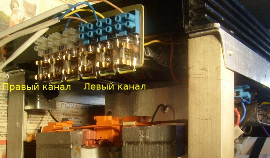
Rear view, with speaker output blocks and fuse box (since no electronic protection circuits were made due to lack of space in the design and in order not to complicate the circuit):
In the future, the frame from the corner is supposed, of course, to be covered with decorative panels to give the product a more “tradeable” look, but this will be done by the “customer” himself, according to his personal taste. But in general, in terms of sound quality and power, the design turned out to be quite decent. Material author: Andrey Baryshev (especially for the site website).
The amp is capable of delivering 2kW of power peak and 1.5kW continuous, which means this amp will burn most speakers you know. To imagine such power in action, you can connect (What I strongly advise against doing) two series-connected 8-ohm speakers to the network alternating current 220V. In this case, on one speaker there will be 110V of the effective voltage on a load of 8 ohms - 1,500W. How long do you think the acoustics will work in this mode. If the desire to deal with this amplifier still has not disappeared, move on ...
Amplifier Description
First, let's look at the requirements to achieve 1.5kW into 4 ohms. We need 77.5V rms, but we need to have some margin because the supply voltage will drop under load and there will always be some voltage drop across the collector-emitter junctions and emitter resistors.
So the voltage should be...
VDC = VRMS * 1.414
VDC = 77.5 * 1.414 = ±109.6V DC voltage
Since we haven't accounted for losses, we need to add about 3-5V to the end of the amplifier, and an additional 10V to the supply voltage drop under full load.
A transformer of 2 x 90V will give an unloaded voltage of ±130V (260V between the ends of the rectifier), so the power supply must be handled with extreme care
Bipolar transistors were selected as the most suitable for the final amplifier stage. This is primarily dictated by the supply voltage, which exceeds boundary stress for most MOSFET transistors. This is also a lot for bipolar transistors, but MJ15004 / 5, or MJ21193 / 4 meet the maximum voltage requirement, and therefore, we will focus on them.
P=V? / R = 65 ? /4=1056W
That is, it is equal to the average electric heater ...
Remember that when driving a resistive load with 45° phase shifts, the power dissipation almost doubles. From this it follows that good cooling vital for this amplifier, you will need good heatsinks, forced cooling fans (natural convection won't help).
MJ15024/5 (or MJ21193/4) transistors in a K-3 package (iron with two leads like KT825/827), and are rated for 250W dissipation at 25°C. The K-3 transistor package is chosen because it has the highest power dissipation rating because the thermal resistance is lower than any other plastic packaged transistor.
The MJE340/350 in the voltage amplifier stage guarantees good linearity. But even with 12mA of current through the stage, the power is 0.72W, so Q4, Q6, Q9 and Q10 must have heatsinks. Transistor (Q5), which determines the bias of the final stage, must be installed on a common radiator with the terminal and have a reliable thermal contact.
The short circuit protection circuit (Q7, Q8) limits the current to 12A and the power dissipated by one transistor to about 175W, while the amplifier is not allowed to operate in this mode for a long time.
1500W professional amplifier circuit.
Additional feedback elements (R6a and C3a, shown in dotted line) are optional. They may be necessary when self-excitation of the amplifier occurs. Freewheel diodes (D9 and D10) protect the amplifier transistors from back EMF when operating on a resistive load. The 1N5404 series diodes can withstand peak current up to 200A. Rated voltage should be at least 400V.
Resistor VR1 100 omo is used to balance the amplifier for DC. With the component values shown in the schematic, the initial offset must be within ±25mV before tuning. Resistor VR2 is used to set the quiescent current of the final stage. Adjust the quiescent current by measuring the voltage across the resistor R19 or R20 which should be within 150mV.
Input stage sensitivity is 1.77V for 900W into 8 ohms, or 1800W into 4 ohms.
Source of power:
The power supply needed for the amplifier requires a serious design approach. First, you need a step-down transformer with a power of at least 2kW. Power filter capacitors must be rated at 150V and withstand up to 10A of ripple current. Capacitors that do not meet these requirements can simply explode when the amplifier is running at full power.
An important detail is the bridge rectifier. Although 35A bridges seem to be up to the task, the peak repetitive current exceeds the bridge ratings. I recommend using two bridges connected in parallel as shown in the diagram. The rated voltage of the bridge rectifier must be at least 400V, and they must be installed with sufficient heat sink for cooling.
Power supply circuit for a 1500W amplifier.
The diagram shows the capacitors made up of four low-voltage ones, since they are easier to find, and the rectifier also consists of two bridges connected in parallel.
Additional voltage sources in 5V can be excluded, while the peak power will decrease from 2048W to 1920W, which is not significant.
The P39 module is a soft start system and consists of a relay whose contacts are connected in parallel with resistors with a total power of 150W and a resulting resistance of 33 ohms.