In this article, we will look at the most basic chip packages that are very often used in everyday electronics.
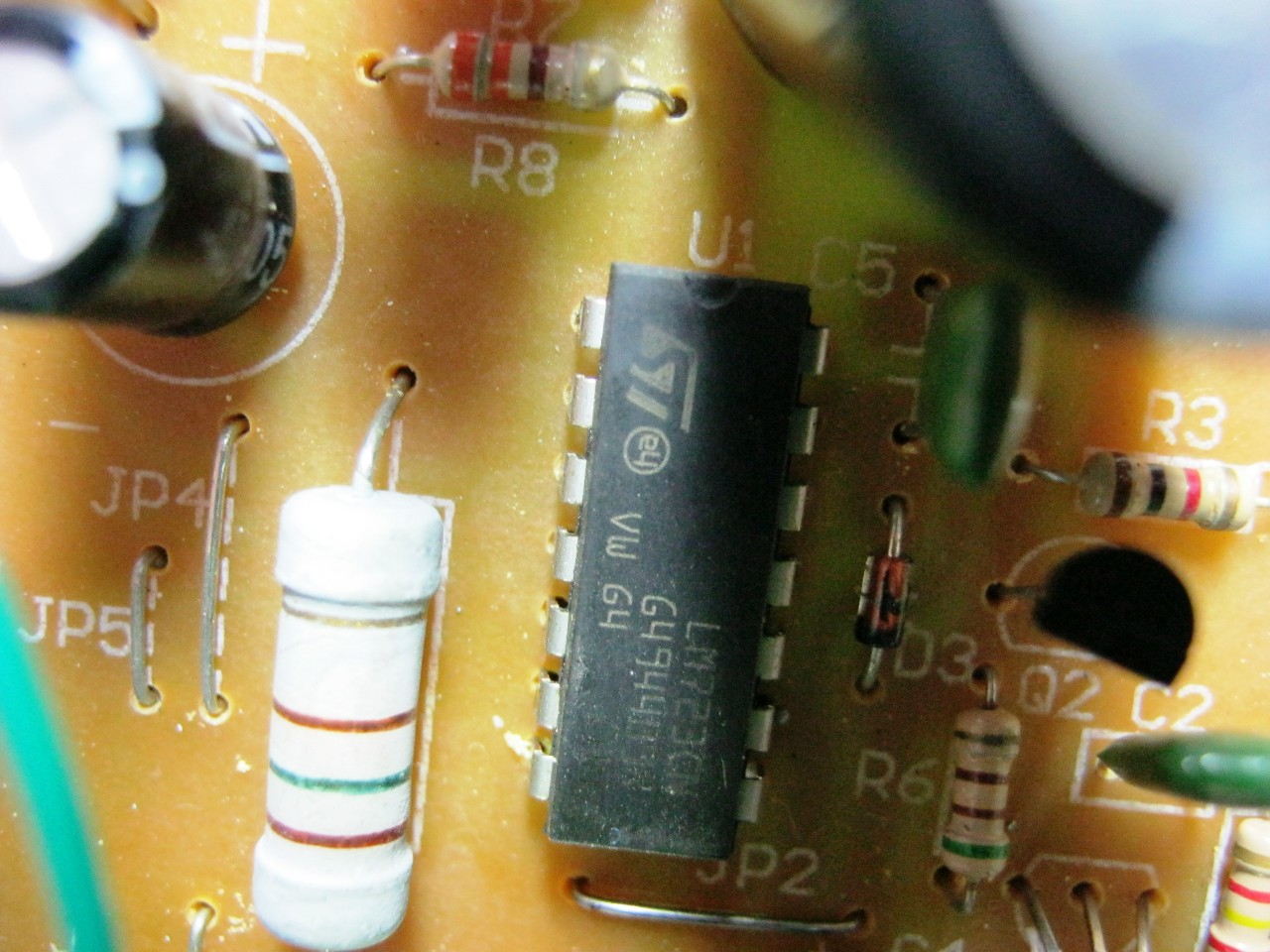
DIP(English) D ual I n line P package)- housing with two rows of leads on the long sides of the microcircuit. Previously, and probably still today, the DIP package was the most popular package for multi-pin microcircuits. It looks like this:


Depending on the number of pins of the microcircuit, the number of its pins is put after the word “DIP”. For example, a microcircuit, or rather, an atmega8 microcontroller, has 28 pins:

Therefore, its package will be called DIP28.
But for this microcircuit, the case will be called DIP16.
Basically, in the DIP package in the Soviet Union, logic microcircuits, operational amplifiers, etc. were produced. Now the DIP package also does not lose its relevance and various microcircuits are still made in it, ranging from simple analog ones to microcontrollers.
The DIP package can be made of plastic (which is the case in most cases) and is called PDIP, as well as from ceramics - CDIP. Feel the body CDIP hard as a stone, and this is not surprising, since it is made of ceramic.
Example CDIP corps.

There are also modificationsHDIP, SDIP.
HDIP (H eat dissipating DIP ) is a heat-dissipating DIP. Such microcircuits pass a large current through themselves, so they get very hot. To remove excess heat, such a microcircuit must have a radiator or its like, for example, as here are two radiator wings in the middle of the mikruha:

SDIP (S mall DIP ) is a small DIP. A microcircuit in a DIP package, but with a small distance between the legs of the microcircuit:

SIP housing
SIP frame ( S angle I n line P ackage) - a flat case with leads on one side. Very easy to install and takes up little space. The number of pins is also written after the package name. For example, mikruha from below in the SIP8 case.

At SIP There are also modifications HSIP(H eat dissipating SIP). That is, the same case, but with a radiator

ZIP case
ZIP ( Z igzag I n line P ackage) - a flat case with leads arranged in a zigzag manner. In the photo below, the ZIP6 case. The number is the number of pins:

Well, the case with a radiator hzip:

We just looked at the main class in-line package microchips. These ICs are designed for through-hole mounting in printed circuit board.
For example, a DIP14 chip installed on a printed circuit board
and its conclusions on the reverse side of the board, already without solder.

Someone still manages to solder DIP chips, like surface mount chips (more on them below), by bending the leads at an angle of 90 degrees, or straightening them completely. This is a perversion), but it works).
Let's move on to another class of microcircuits - surface mount chips or the so-called SMD components. They are also called planar radio components.
Such microcircuits are soldered on the surface of the printed circuit board, under the printed conductors allocated for them. See the rectangular tracks in a row? These are printed conductors or among the people patches. It is precisely on them that planar microcircuits are soldered.


SOIC package
The largest representative of this class of microcircuits are microcircuits in a package. SOIC (S mall- O utline I integrated C ircuit) - a small microcircuit with leads on the long sides. It is very similar to DIP, but pay attention to its conclusions. They are parallel to the surface of the case itself:

This is how they are soldered on the board:

Well, as usual, the number after “SOIC” indicates the number of pins of this microcircuit. In the photo above, the chips are in the SOIC16 package.
SOP (S mall O utline P ackage) is the same as SOIC.

SOP body modifications:
PSOP– plastic housing SOP. It is the one most often used.
HSOP– heat dissipating SOP. Small radiators in the middle serve to remove heat.

SSOP(S hrink S mall O utline P package)– “wrinkled” SOP. That is even smaller than the SOP enclosure

TSSOP(T hin S hrink S mall O utline P package)– thin SSOP. The same SSOP, but “smeared” with a rolling pin. Its thickness is less than that of SSOP. Basically, in the TSSOP package, microcircuits are made that decently heat up. Therefore, the area of such microcircuits is larger than that of conventional ones. In short, the case-radiator).

SOJ- the same SOP, but the legs are bent in the shape of a letter "J" under the microchip. In honor of such legs, the SO case was named J:

Well, as usual, the number of pins is indicated after the package type, for example, SOIC16, SSOP28, TSSOP48, etc.
QFP package
QFP (Q uad F lat P package)- rectangular flat body. The main difference from the fellow SOIC is that the findings are placed on all sides of such a chip

Modifications:
PQFP– QFP plastic case. CQFP- Ceramic QFP package. HQFP– heat-dissipating QFP housing.
TQFP (T hin Q uad F lat P ack)- Slim QFP package. Its thickness is much less than that of its QFP counterpart.


PLCC (P elastic L headed C hip C arrier) and CLCC (C eramic L headed C hip C arrier)- respectively, a plastic and ceramic case with contacts located at the edges, designed for installation in a special socket, popularly called a “crib”. A typical representative is the BIOS chip in your computers.

This is what the “crib” looks like for such microcircuits

And this is how the microcircuit “lies” in the crib.

Sometimes these chips are called QFJ, you guessed it, because of the letter-shaped pins "J"
Well, the number of pins is placed after the package name, for example PLCC32.
PGA package
PGA (P in G rid A array)- a matrix of pins. It is a rectangular or square case, in the lower part of which there are pins

Such microcircuits are also installed in special beds, which clamp the microcircuit pins with a special lever.

In the PGA package, they mainly make processors for your personal computers.
LGA case
LGA (L and G rid A rray) - a type of microcircuit packages with a matrix of contact pads. Most often used in computer technology for processors.
The bed for LGA chips looks something like this:

If you look closely, you can see spring-loaded contacts.
The microcircuit itself, in this case the PC processor, has simply metallized pads:

In order for everything to work, a condition must be met: the microprocessor must be tightly pressed against the crib. For this, various types of latches are used.
BGA package
BGA (B all G rid A ray) is a matrix of balls.

As we can see, here the leads are replaced by solder balls. On one such microcircuit, hundreds of lead balls can be placed. The board space savings are fantastic. Therefore, microcircuits in the BGA package are used in the production of mobile phones, tablets, laptops and other microelectronic devices. I also wrote about how to solder BGA in the article Soldering BGA chips.
In the red squares, I marked the microcircuits in the BGA package on the board mobile phone. As you can see, now all microelectronics are built on BGA microcircuits.

BGA technology is the apogee of microelectronics. At present, the world has already switched to the technology of microBGA packages, where the distance between the balls is even smaller, and you can even fit thousands (!) of pins under one chip!
So we have dismantled the main cases of microcircuits.
There is nothing wrong with calling a chip in a SOIC package SOP or SOP SSOP. There is also nothing wrong with calling the QFP case TQFP. The boundaries between them are blurred and these are just conventions. But if you call a microcircuit in a BGA package DIP, then this will already be a complete fiasco.
Beginning radio amateurs should just remember the three most important packages for microcircuits - these are DIP, SOIC (SOP) and QFP without any modifications, and it is also worth knowing their differences. Basically, it is these types of chip packages that radio amateurs use most often in their practice.
There are two test methods for diagnosing a fault. electronic system, device or printed circuit board: functional control and in-circuit control. Functional control checks the operation of the module under test, and in-circuit control consists in checking individual elements of this module in order to find out their ratings, polarity, etc. Usually, both of these methods are applied sequentially. With the development of automatic control equipment, it became possible to very quickly in-circuit control with an individual check of each element of the printed circuit board, including transistors, logic elements and counters. Functional control has also moved to a new qualitative level due to the use of computer data processing and computer control methods. As for the principles of troubleshooting themselves, they are exactly the same, regardless of whether the check is carried out manually or automatically.
Troubleshooting must be carried out in a certain logical sequence, the purpose of which is to find out the cause of the malfunction and then eliminate it. The number of operations performed should be kept to a minimum, avoiding unnecessary or meaningless checks. Before checking a faulty circuit, you need to carefully inspect it for possible detection of obvious defects: burned out elements, breaks in conductors on a printed circuit board, etc. This should be given no more than two to three minutes, with the acquisition of experience such visual control will be performed intuitively. If the inspection did not give anything, you can proceed to the troubleshooting procedure.
First of all, it is performed functional test: the operation of the board is checked and an attempt is made to determine the faulty block and the suspected faulty element. Before replacing a defective element, you must carry out in-circuit measurement parameters of this element in order to verify its malfunction.
Functional Tests
Functional tests can be divided into two classes, or series. Tests series 1, called dynamic tests, applied to completed electronic device to isolate a faulty stage or block. When the specific block with which the fault is associated is found, tests are applied series 2, or static tests, to identify one or two possibly faulty elements (resistors, capacitors, etc.).
Dynamic tests
This is the first set of tests performed when troubleshooting an electronic device. Troubleshooting should be carried out in the direction from the output of the device to its input along bisection method. The essence of this method is as follows. First, the entire circuit of the device is divided into two sections: input and output. A signal is applied to the input of the output section, similar to the signal that, under normal conditions, acts at the split point. If at the same time a normal signal is obtained at the output, then the fault must be in the input section. This input section is divided into two subsections and the previous procedure is repeated. And so on, until the fault is localized in the smallest functionally distinct stage, for example, in the output stage, video amplifier or IF amplifier, frequency divider, decoder, or a separate logic element.
Example 1. Radio receiver (Fig. 38.1)
The most suitable first division of the radio receiver circuit is the division into the AF section and the IF / RF section. First, the AF section is checked: a signal with a frequency of 1 kHz is fed to its input (volume control) through an isolation capacitor (10-50 uF). Weak or distorted signal, as well as its complete absence indicate a malfunction of the AF section. We now divide this section into two subsections: the output stage and the preamplifier. Each subsection is checked starting from the output. If the AF section is OK, then a clear tone signal (1 kHz) should be heard from the loudspeaker. In this case, the fault must be sought inside the IF / RF section.
Rice. 38.1.
You can very quickly verify the serviceability or malfunction of the AF section using the so-called "screwdriver" test. Touch the end of a screwdriver to the input terminals of the AF section (after setting the volume control to maximum volume). If this section is OK, the loudspeaker hum will be clearly audible.
If the fault is found to be within the IF/RF section, it should be divided into two subsections: the IF section and the RF section. First, the IF section is checked: an amplitude-modulated (AM) signal with a frequency of 470 kHz 1 is fed to its input, i.e., to the base of the transistor of the first IF, through a decoupling capacitor with a capacitance of 0.01-0.1 μF. FM receivers require a 10.7 MHz frequency modulated (FM) test signal. If the IF section is OK, a clean tone (400-600 Hz) will be heard through the loudspeaker. Otherwise, the IF partitioning procedure should be continued until the faulty stage, such as an IF or a detector, is found.
If the fault is within an RF section, then the section is split into two subsections, if possible, and checked as follows. An AM signal with a frequency of 1000 kHz is fed to the input of the cascade through a decoupling capacitor with a capacity of 0.01-0.1 μF. The receiver is tuned to receive a radio signal with a frequency of 1000 kHz, or a wavelength of 300 m in the medium wave band. In the case of an FM receiver, a test signal of a different frequency is naturally required.
You can also use an alternative verification method - method of cascading verification of the signal passage. The radio turns on and tunes in to a station. Then, starting from the output of the device, using an oscilloscope, the presence or absence of a signal at the control points is checked, as well as the compliance of its shape and amplitude with the required criteria for a working system. When troubleshooting in any other electronic device, a nominal signal is applied to the input of this device.
The considered principles of dynamic tests can be applied to any electronic device, provided that the system is properly partitioned and the parameters of the test signals are selected.
Example 2. Digital divider and display (Fig. 38.2)
As can be seen from the figure, the first test is performed at the point where the circuit is divided into approximately two equal parts. To change the logical state of the signal at the input of block 4, a pulse generator is used. The Light Emitting Diode (LED) at the output should change state if the latch, amplifier, and LED are OK. Further troubleshooting should be continued in the dividers preceding block 4. The same procedure is repeated using the pulse generator until the faulty divider is determined. If the LED does not change state in the first test, then the fault is in blocks 4, 5, or 6. Then the pulse generator signal should be applied to the input of the amplifier, etc.

Rice. 38.2.
Principles of static tests
This series of tests is used to determine the defective element in the cascade, the failure of which was established at the previous stage of checks.
1. Start by checking static modes. Use a voltmeter with a sensitivity of at least 20 kOhm/V.
2. Measure voltage only. If you want to determine the amount of current, calculate it by measuring the voltage drop across a resistor of known value.
3. If measurements at direct current did not reveal the cause of the malfunction, then and only then proceed to dynamic testing of the faulty stage.
Testing a single-stage amplifier (Fig. 38.3)
Typically, the nominal values of constant voltages in control points cascade are known. If not, they can always be estimated with acceptable accuracy. By comparing the actual measured voltages with their nominal values, you can find a defective element. First of all, the static mode of the transistor is determined. There are three options here.
1. The transistor is in a cutoff state, not producing any output signal, or in a state close to cutoff (“goes” into the cutoff region in dynamic mode).
2. The transistor is in saturation, producing a weak distorted output signal, or in a state close to saturation ("goes" into saturation in dynamic mode).
$11. Transistor in normal static mode.

Rice. 38.3. Rated voltages:
V e = 1.1 V, V b = 1.72 V, V c = 6.37V.
Rice. 38.4. Open resistor R 3, transistor
is in cutoff state: V e = 0.3V
V b = 0.94V V c = 0.3V.
After installed real mode operation of the transistor, it turns out the cause of the cutoff or saturation. If the transistor is operating in normal static mode, the fault is related to the passage of an AC signal (such a fault will be discussed later).
cutoffThe cut-off mode of the transistor, i.e., the cessation of current flow, occurs when a) the base-emitter junction of the transistor has zero bias voltage or b) the current flow path is broken, namely: when the resistor breaks (burns out) R 3 or resistor R 4 or when the transistor itself is faulty. Normally, when the transistor is in the cutoff state, the collector voltage is equal to the power supply voltage V CC . However, if the resistor breaks R 3 collector "floats" and theoretically should have the potential of the base. If you connect a voltmeter to measure the voltage across the collector, the base-collector junction is in forward bias conditions, as seen in Fig. 38.4. In the circuit "resistor R 1 - base-collector junction - voltmeter "current will flow, and the voltmeter will show a small amount of voltage. This reading is entirely related to the internal resistance of the voltmeter.
Likewise, when the cutoff is caused by an open resistor R 4, the emitter of the transistor "floats", which theoretically should have the base potential. If you connect a voltmeter to measure the voltage at the emitter, a current flow circuit is formed with a forward biased base-emitter junction. As a result, the voltmeter will show a voltage slightly higher than the nominal voltage at the emitter (Fig. 38.5).
In table. 38.1 summarizes the faults discussed above.

Rice. 38.5.Open resistorR 4, transistor
is in cutoff state:
V e = 1.25 V, V b = 1.74 V, V c = 10 V.
Rice. 38.6.Transition short circuit
base-emitter, the transistor is in
cut-off state:V e = 0.48 V, V b = 0.48 V, V c = 10 V.
Note that the term "high V BE " means the excess of the normal forward bias voltage of the emitter junction by 0.1 - 0.2 V.
Transistor failure also creates cutoff conditions. The voltages at the control points depend in this case on the nature of the fault and the ratings of the circuit elements. For example, a short circuit of the emitter junction (Fig. 38.6) leads to the current cutoff of the transistor and the parallel connection of resistors R 2 and R 4 . As a result, the potential of the base and emitter is reduced to a value determined by the voltage divider R 1 – R 2 || R 4 .
Table 38.1. Cutoff conditions
|
Malfunction |
Cause |
|
V b V c V BE |
vac |
Open resistor R 1 |
V b V c V BE |
High Normal V CC Low |
Open resistor R 4 |
V b V c V BE |
Low Low Low Normal |
Open resistor R 3 |
In this case, the collector potential is obviously equal toV CC . On fig. 38.7 considers the case of a short circuit between the collector and the emitter.
Other cases of transistor failure are given in Table. 38.2.

Rice. 38.7.Short circuit between collector and emitter, transistor is in cutoff state:V e = 2.29 V, V b = 1.77 V, V c = 2.29 V.
Table 38.2
|
Malfunction |
Cause |
|
V b V c V BE |
0 Normal V CC Very high, cannot be sustained by functioning pn-transition |
Breaking the base-emitter junction |
V b V c V BE |
Low Low V CC Normal |
Discontinuity of base-collector junction |
As explained in ch. 21, the transistor current is determined by the forward bias voltage of the base-emitter junction. A small increase in this voltage leads to a strong increase in the current of the transistor. When the current through the transistor reaches its maximum value, the transistor is said to be saturated (is in a state of saturation). Potential
Table 38.3
|
Malfunction |
Cause |
|
V b V c |
High ( V c) high Low |
Open resistor R 2 or low resistance resistorR 1 |
V b V c |
Low Very low |
Capacitor short circuitC 3 |
collector decreases with increasing current and when saturation is reached, it is practically equal to the emitter potential (0.1 - 0.5 V). In general, at saturation, the potentials of the emitter, base, and collector are approximately at the same level (see Table 38.3).
Normal static modeThe coincidence of the measured and nominal DC voltages and the absence or low level of the signal at the output of the amplifier indicate a malfunction associated with the passage of the AC signal, for example, an internal open in the coupling capacitor. Before replacing a suspected open capacitor, make sure it is faulty by connecting a serviceable capacitor of close rating in parallel with it. Break of the decoupling capacitor in the emitter circuit ( C 3 in the diagram in fig. 38.3) leads to a decrease in the signal level at the output of the amplifier, but the signal is reproduced without distortion. A large leakage or short circuit in this capacitor will usually change the transistor's mode according to direct current. These changes depend on the static modes of the previous and subsequent stages.
When troubleshooting, keep the following in mind.
1. Do not jump to conclusions based on a comparison of the measured and rated voltage only at one point. It is necessary to record the entire set of measured voltages (for example, at the emitter, base and collector of the transistor in the case of a transistor stage) and compare it with a set of corresponding nominal voltages.
2. With accurate measurements (for a voltmeter with a sensitivity of 20 kOhm / V, an accuracy of 0.01 V is achievable), two identical readings at different control points in the vast majority of cases indicate a short circuit between these points. However, there are exceptions, so you need to perform all further checks for the final conclusion.
Features of diagnostics of digital circuits
In digital devices, the most common malfunction is the so-called “sticking”, when a logic 0 (“constant zero”) or logic 1 (“constant one”) level is constantly on the output of the IC or in a circuit node. Other failures are also possible, including breaks in the IC leads or a short circuit between the PCB traces.

Rice. 38.8.
Diagnostics of faults in digital circuits is carried out by applying the signals of a logical pulse generator to the inputs of the element under test and observing the effect of these signals on the state of the outputs using a logical probe. For a complete check of a logical element, its entire truth table is “passed”. Consider, for example, digital circuit in fig. 38.8. First, the logical states of the inputs and outputs of each logic element are recorded and compared with the states in the truth table. A suspicious logic element is tested using a pulse generator and a logic probe. Consider, for example, the logical element G 1 . At its input 2, the logic level 0 is constantly active. To check the element, the generator probe is installed at pin 3 (one of the two inputs of the element), and the probe probe is at pin 1 (element output). Referring to the truth table of the OR NOT element, we see that if one of the inputs (pin 2) of this element has a logical level of 0, then the signal level at its output changes when the logical state of the second input (pin 3) changes.
Element truth tableG 1
|
Conclusion 2 |
Conclusion 3 |
Conclusion 1 |
For example, if in original state logical 0 acts on pin 3, then there is a logical 1 at the output of the element (pin 1). If now using the generator to change the logical state of pin 3 to logical 1, then the output signal level will change from 1 to 0, which will register the probe. The opposite result is observed when, in the initial state, a logic level of 1 acts on pin 3. Similar tests can be applied to other logic elements. In these tests, it is imperative to use the truth table of the logical element being tested, because only in this case can one be sure of the correctness of testing.
Features of diagnostics of microprocessor systems
Troubleshooting in a microprocessor system with a bus structure takes the form of sampling the sequence of addresses and data that appear on the address bus and data bus, and then comparing them to a well-known sequence for a running system. For example, a fault such as a hard 0 on line 3 (D 3 ) of the data bus would be indicated by a hard logical zero on line D 3 . The corresponding listing, called status listing, obtained using a logic analyzer. A typical status listing displayed on the monitor screen is shown in fig. 38.9. Alternatively, a signature analyzer can be used to collect a bit stream, called a signature, at some node in the circuit and compare it to a reference signature. The difference in these signatures indicates a malfunction.

Rice. 38.9.
This video is about a computer tester for troubleshooting personal computers IBM PC type:
Good day dear radio amateurs!
I welcome you to the site ""
Microcircuits
Chip (IC - Integrated Circuit, IC - Integrated Circuit, chip or microchip from English Chip, Microchip) is a whole device containing transistors, diodes, resistors and other active and passive elements, total number which can reach several tens, hundreds, thousands, tens of thousands and more. There are many types of microcircuits. The most used among them are brain teaser, operational amplifiers, specialized.
Most of the microcircuits are housed in a rectangular plastic package with flexible plate leads (see Fig. 1) located along both sides of the package. On top of the case there is a conditional key - a round or other form of label, from which the pins are numbered. If you look at the microcircuit from above, then you need to count the conclusions counterclockwise, and if from below, then in the clockwise direction. Chips can have any number of pins.
In domestic electronics (however, in foreign too), microcircuits are especially popular brain teaser, built on the basis of bipolar transistors and resistors. They are also called TTL chips (TTL - Transistor-Transistor Logic). The name transistor-transistor came from the fact that transistors are used both to perform logic functions and to amplify the output signal. Their entire principle of operation is built on two conditional levels: low or high, or, equivalently, the state of logical 0 or logical 1. So, for K155 series microcircuits, voltages from 0 to 0.4 are taken as a low level corresponding to logical 0. V, that is, not more than 0.4 V, and for high, corresponding to logical 1, - not less than 2.4 V and not more than the power supply voltage - 5 V, and for K176 series microcircuits designed to be powered from a source, a voltage of 9 B, respectively 0.02. ..0.05 and 8.6. ..8.8 V.
Marking of foreign TTL microcircuits begins with the numbers 74, for example 7400. Conventional graphic designations of the main elements of logical microcircuits are shown in Fig. 2. There are also truth tables that give an idea of the logic of these elements.

The symbol of the logical element AND is the sign “&”(conjunction "and" in English language) standing inside the rectangle (see Fig.2). On the left are two (or more) input pins, on the right is one output pin. The logic of this element is as follows: a high-level voltage will appear at the output only when signals of the same level are at all its inputs. The same conclusion can be drawn by looking at the truth table characterizing the electrical state of the AND element and the logical connection between its output and input signals. So, for example, in order for the output (Out.) of the element to have a high-level voltage, which corresponds to a single (1) state of the element, both inputs (In. 1 and In. 2) must have voltages of the same level. In all other cases, the element will be in the zero (0) state, that is, a low-level voltage will operate at its output.
Conditional Boolean Symbol OR- number 1
in a rectangle. It, like the AND element, can have two or more inputs. The output signal corresponding to a high level (logic 1) appears when a signal of the same level is applied to input 1 or input 2, or simultaneously to all inputs. Check these logical relationships of the output and input signals of this element against its truth table.
Conditional element symbol NOT- also a number 1
inside the rectangle. But it has one entrance and one exit. A small circle, which begins the output signal line, symbolizes the logical negation of “NOT” at the output of the element. In the language of digital technology, “NOT” means that the element is NOT an inverter, that is, an electronic “brick”, the output signal of which is opposite in level to the input. In other words: as long as there is a low level signal at its input, the output will be a high level signal, and vice versa. This is also indicated by the logical levels in the truth table of the operation of this element.
Logic element AND-NOT is a combination of elements And and NOT, therefore, on its conditional graphic designation there is a sign “ &
” and a small circle on the output signal line, symbolizing logical negation. There is only one exit, but two or more entrances. The logic of the element is as follows: a high-level signal appears at the output only when there are low-level signals at all inputs. If at least one of the inputs has a low-level signal, the output of the AND-NOT element will have a high-level signal, that is, it will be in a single state, and if there is a high-level signal at all inputs, it will be in the zero state. The AND-NOT element can perform the function of the NOT element, that is, become an inverter. To do this, you just need to connect together all its inputs. Then, when a low-level signal is applied to such a combined input, the output of the element will be a high-level signal, and vice versa. This property of the AND-NOT element is very widely used in digital technology.
Symbol designation logical elements(signs “&” or “1”) is used only in domestic circuitry.
TTL microcircuits provide the construction of a wide variety of digital devices operating at frequencies up to 80 MHz, but their significant drawback is their high power consumption.
In some cases, when high performance is not needed, but minimum power consumption required, CMOS chips are used, which are used FETs and not bipolar. Reduction CMOS (CMOS Complementary Metal-Oxide Semiconductor) stands for Complementary Metal Oxide Semiconductor. The main feature of CMOS microcircuits is negligible current consumption in static mode - 0.1 ... 100 μA. When operating at the maximum operating frequency, the power consumption increases and approaches the power consumption of the least powerful TTL chips. CMOS microcircuits include such well-known series as K176, K561, KR1561 and 564.
In class analog chips isolated microcircuits with linear characteristics - linear microcircuits, which include OU – Operational Amplifiers. Name " operational amplifier” is due to the fact that, first of all, such amplifiers have been used to perform operations of summing signals, their differentiation, integration, inversion, etc. Analog microcircuits are produced, as a rule, functionally unfinished, which opens up wide scope for amateur radio creativity.

Operational amplifiers have two inputs - inverting and non-inverting. In the diagram, they are indicated by minus and plus, respectively (see Fig. 3). By applying a signal to the input plus - the output is unchanged, but amplified signal. By applying it to the minus input, the output is an inverted, but also amplified signal.
In the production of radio electronic products the use of multifunctional specialized microcircuits that require a minimum number of external components can significantly reduce the development time of the final device and production costs. This category of chips includes chips that are designed for something specific. For example, there are microcircuits for power amplifiers, stereo receivers, and various decoders. All of them can have a completely different look. If one of these microcircuits has a metal part with a hole, this means that it must be screwed to
radiator.
Dealing with specialized microcircuits is much more pleasant than with a mass of transistors and resistors. If earlier it was necessary to assemble a radio receiver with a lot of parts, now you can get by with one microcircuit.
Electronics accompanies modern man everywhere: at work, at home, in the car. Working in production, and no matter in what particular area, you often have to repair something electronic. Let's agree to call this "something" a "device". This is such an abstract collective image. Today we’ll talk about all kinds of repair wisdom, having mastered which, you can repair almost any electronic “device”, regardless of its design, principle of operation and scope.
Where to begin
There is little wisdom in resoldering a part, but finding a defective element is the main task in repair. You should start by determining the type of malfunction, since it depends on where to start the repair.
There are three such types:
1. the device does not work at all - the indicators do not light up, nothing moves, nothing buzzes, there are no responses to the control;
2. any part of the device does not work, that is, part of its functions is not performed, but although glimpses of life in it are still visible;
3. The device mostly works properly, but sometimes it makes so-called failures. It is impossible to call such a device broken yet, but still something prevents it from working normally. Repair in this case just consists in finding this interference. It is believed that this is the most difficult repair.
Let's look at examples of repairing each of the three types of faults.
Repair of the first category
Let's start with the simplest - a breakdown of the first type, this is when the device is completely dead. Anyone will guess that you need to start with nutrition. All devices living in their own world of machines necessarily consume energy in one form or another. And if our device does not move at all, then the probability of the absence of this very energy is very high. A small digression. When looking for a fault in our device, we will often talk about “probability”. Repair always begins with the process of determining possible points of influence on the malfunction of the device and estimating the probability of involvement of each such point in this particular defect, with the subsequent transformation of this probability into a fact. At the same time, do the right thing, that is, with the most a high degree The most complete knowledge of the device device, its operation algorithm, the physical laws on which the device is based, the ability to think logically and, of course, His Majesty experience will help to assess the probability of the influence of any block or node on the problems of the device. One of the most effective repair methods is the so-called elimination method. From the entire list of all blocks and assemblies suspected of involvement in the defect of the device, with varying degrees of probability, it is necessary to consistently exclude the innocent.
It is necessary to start the search, respectively, from those blocks, the probability of which may be the culprits of this malfunction is the highest. Hence, it turns out that the more precisely this very degree of probability is determined, the less time will be spent on repairs. In modern "devices" internal nodes are strongly integrated with each other, and there are a lot of connections. Therefore, the number of points of influence is often extremely large. But your experience is also growing, and over time you will identify the "pest" with a maximum of two or three attempts.
For example, there is an assumption that with a high probability block “X” is to blame for the illness of the device. Then you need to conduct a series of checks, measurements, experiments that would confirm or disprove this assumption. If after such experiments even the slightest doubt remains that the block was not involved in the “criminal” influence on the device, then this block cannot be completely excluded from the number of suspects. It is necessary to look for such a way to check the suspect's alibi in order to be 100% sure of his innocence. This is very important in the elimination method. And the most reliable way such a check of the suspect is the replacement of the unit with a known good one.
Let's get back to our "patient", in whom we assumed a power failure. Where to start in this case? And as in all other cases - with a complete external and internal examination of the "patient". Never neglect this procedure, even when you are sure that you know the exact location of the breakdown. Inspect the device always completely and very carefully, slowly. Often, during the inspection, you can find defects that do not directly affect the problem you are looking for, but which can cause a breakdown in the future. Look for burnt electrical components, swollen capacitors, and other suspicious looking items.
If the external and internal examination did not bring any results, then pick up a multimeter and get to work. I hope there is no need to remind about checking the presence of mains voltage and fuses. But let's talk a little about power supplies. First of all, check the high-energy elements of the power supply (PSU): output transistors, thyristors, diodes, power microcircuits. Then you can start to sin on the remaining semiconductors, electrolytic capacitors and, last but not least, on the rest of the passive electrical elements. In general, the value of the probability of failure of an element depends on its energy saturation. The more energy an electrical element uses for its functioning, the more likely it is to break.
If mechanical components are worn out by friction, then electrical ones are worn out by current. The greater the current, the greater the heating of the element, and heating / cooling wears out any materials no worse than friction. Temperature fluctuations lead to deformation of the material of electrical elements at the micro level due to thermal expansion. Such variable temperature loads are the main cause of the so-called material fatigue effect during the operation of electrical elements. This must be taken into account when determining the order in which elements are checked.
Do not forget to check the PSU for output voltage ripples, or any other interference on the power buses. Although infrequently, such defects can also cause the device to fail. Check whether the power actually reaches all consumers. Maybe due to problems in the connector / cable / wire, this “food” does not reach them? The PSU will be serviceable, but there is still no energy in the device blocks.
It also happens that a malfunction lurks in the load itself - a short circuit (short circuit) is not uncommon there. At the same time, in some “economical” PSUs there is no current protection and, accordingly, there is no such indication. Therefore, the version of the short circuit in the load should also be checked.

Now the failure of the second type. Although here too everything should start with the same external-internal examination, there is a much greater variety of aspects to which attention should be paid. - The most important thing is to have time to remember (write down) the whole picture of the state of the sound, light, digital indication of the device, error codes on the monitor, display, the position of alarms, flags, blinkers at the time of the accident. Moreover, it is obligatory before its reset, acknowledgment, power off! It is very important! miss some important information- means by all means to increase the time spent on repairs. Examine all the available indications - both emergency and working, and remember all the indications. Open the control cabinets and memorize (write down) the state of the internal indication, if any. Shake the boards installed on the motherboard, cables, blocks in the device case. Maybe the problem will go away. And be sure to clean the radiators.
Sometimes it makes sense to check the voltage on some suspicious indicator, especially if it is an incandescent lamp. Carefully read the readings of the monitor (display), if available. Decipher the error codes. Look at the tables of input and output signals at the time of the accident, write down their status. If the device has the function of recording the processes occurring with it, do not forget to read and analyze such an event log.
Feel free to sniff the device. Is there a characteristic smell of burnt insulation? Pay special attention to products made of carbolite and other reactive plastics. Infrequently, but it happens that they break through, and this breakdown is sometimes very hard to see, especially if the insulator is black. Due to their reactive properties, these plastics do not warp when heated, which also makes it difficult to detect broken insulation.
Look for darkened insulation of relay windings, starters, electric motors. Are there any darkened resistors and other electrical radio elements that have changed their normal color and shape.
Are there any bulging or "shooting" capacitors.
Check if there is water, dirt, foreign objects in the device.
See if the connector is skewed, or if the block/board is not fully inserted into its place. Try removing and reinserting them.
Perhaps some switch on the device is in the wrong position. The button is stuck, or the moving contacts at the switch have become in an intermediate, not fixed position. Perhaps the contact has disappeared in some toggle switch, switch, potentiometer. Touch them all (when the device is de-energized), move it, turn it on. It won't be redundant.
Check the mechanical parts of the actuators for jamming - turn the rotors of the electric motors, stepper motors. Move other mechanisms as needed. Compare the effort applied in this case with other similar working devices, if of course there is such a possibility.
Inspect the inside of the device while it is running - you may see strong sparking in the contacts of relays, starters, switches, which will indicate an excessively high current in this circuit. And this is a good clue for troubleshooting. Often the fault of such a breakdown is a defect in a sensor. These intermediaries between the outside world and the device they serve are usually placed far beyond the edge of the device body itself. And at the same time, they usually work in a more aggressive environment than the internal parts of the device, which, one way or another, are protected from external influences. Therefore, all sensors require increased attention to themselves. Check their performance and do not be too lazy to clean them from contamination. Limit switches, various blocking contacts and other sensors with galvanic contacts are high priority suspects. And in general, any "dry contact" i.e. not soldered, should become an element of close attention.
And another point - if the device has already served for a long time, then you should pay attention to the elements that are most susceptible to any wear or change in their parameters over time. For example: mechanical components and parts; elements exposed during operation to increased heat or other aggressive effects; electrolytic capacitors, some types of which tend to lose capacity over time due to the drying of the electrolyte; all contact connections; instrument controls.
Almost all types of "dry" contacts lose their reliability over time. Special attention should be paid to silver plated contacts. If the device for a long time worked without maintenance, I recommend that before starting an in-depth troubleshooting, do preventive maintenance of contacts - brighten them with an ordinary eraser and wipe with alcohol. Attention! Never use abrasive pads to clean silver or gold plated contacts. This is certain death to the connector. The coating with silver or gold is always done in a very thin layer, and it is very easy to erase it with an abrasive to copper. It is useful to carry out the self-cleaning procedure for the contacts of the female part of the connector, in the professional slang of “mother”: connect and disconnect the connector several times, the springy contacts are slightly cleaned of friction. I also advise, when working with any contact connections, do not touch them with your hands - oil stains from fingers negatively affect the reliability of electrical contact. Cleanliness is the key to reliable operation of the contact.
The first thing is to check the operation of any blocking, protection at the beginning of the repair. (In any normal technical documentation for the device there is a chapter with detailed description locks applied to it.)
After inspecting and checking the power, think offhand - what is most likely broken in the device, and check these versions. Immediately into the jungle of the device is not worth climbing. First, check all the peripherals, especially the serviceability of the executive bodies - perhaps it was not the device itself that broke, but some mechanism controlled by it. In general, it is recommended to study, albeit not to the subtleties, the entire production process, in which the ward device is a participant. When the obvious versions are exhausted - then sit down at your desktop, make some tea, lay out the diagrams and other documentation for the device and “give birth” to new ideas. Think about what else could cause this disease of the device.
After some time, you should "be born" a certain number of new versions. Here I recommend not to rush to run to check them. Sit down somewhere in a calm atmosphere and think over these versions in terms of the magnitude of the probability of each of them. Train yourself in assessing such probabilities, and when you gain experience in such selection, you will begin to make repairs much faster.
The most effective and reliable way to test a suspected unit, a device node for operability, as already mentioned, is to replace it with a known good one. Do not forget to carefully check the blocks for their complete identity. If you connect the unit under test to a device that is working properly, then, if possible, make sure - check the unit for excessive output voltages, a short circuit in the power supply and in the power section, and others possible faults which could damage the device. The reverse also happens: you connect a donor working board to a broken device, check what you wanted, and when you return it back, it turns out to be inoperative. This does not happen often, but still keep this point in mind.
If in this way it was possible to find a faulty unit, then the so-called “signature analysis” will help to further localize the troubleshooting to a specific electrical element. This is the name of the method in which the repairman conducts an intellectual analysis of all the signals with which the tested node “lives”. Connect the block, node, board under study to the device using special extension adapters (these are usually supplied with the device) so that there is free access to all electrical elements. Lay out the diagram side by side measuring instruments and turn on the power. Now check the signals at the control points on the board with the voltages, waveforms on the diagram (in the documentation). If the scheme and documentation do not shine with such details, strain your brains here. A good knowledge of circuitry will be very useful here.
If there are any doubts, then you can “hang” a serviceable exemplary board from a working device on the adapter and compare the signals. Check with the circuit (with documentation) all possible signals, voltages, waveforms. If a deviation of any signal from the norm is found, do not rush to conclude that this particular electrical element is malfunctioning. It may not be the cause, but just a consequence of another abnormal signal that forced this element to issue a false signal. During repairs, try to narrow the search circle, to localize the malfunction as much as possible. When working with a suspect node / block, come up with such tests and measurements for it that would exclude (or confirm) the involvement of this node / block in this malfunction for sure! Think seven times when you exclude a block from the number of unreliable ones. All doubts in this case must be dispelled by clear evidence.
Always make experiments meaningfully, the “scientific poke” method is not our method. Say, let me stick this wire here and see what happens. Never be like such "repairers". The consequences of any experiment must necessarily be thought out and carried useful information. Pointless experiments - Waste time, and besides, something else can be broken. Develop the ability to think logically, strive to see clear cause-and-effect relationships in the operation of the device. Even the operation of a broken device has its own logic, there is an explanation for everything. You will be able to understand and explain the non-standard behavior of the device - you will find its defect. In the matter of repair, it is very important to clearly imagine the algorithm of the device. If you have gaps in this area, read the documentation, ask everyone who knows at least something about the issue of interest. And do not be afraid to ask, contrary to popular belief, this does not diminish authority in the eyes of colleagues, but on the contrary, smart people will always appreciate it positively. It is absolutely unnecessary to memorize the scheme of the device; paper was invented for this. But the algorithm of its work must be known "by heart". And now you have been “shaking” the device for many days. We studied it so that it seems there is nowhere further. And already repeatedly tortured all suspected blocks / nodes. Even the seemingly most fantastic options have been tried, but the malfunction has not been found. You are already starting to get a little nervous, maybe even panic. Congratulations! You have reached the apogee in this repair. And here only ... rest will help! You're just tired, you need to take a break from work. You have, as experienced people say, "the eye is washed out." So stop working and completely turn off your attention from the ward device. You can do something else, or do nothing at all. But you need to forget about the device. But when you rest, you yourself will feel the desire to continue the battle. And as often happens, after such a break, you suddenly see such a simple solution to the problem that you will be surprised beyond words!

But with a malfunction of the third type, everything is much more complicated. Since failures in the operation of the device are usually random in nature, it often takes a lot of time to catch the moment of manifestation of a failure. The features of the external examination in this case are to combine the search for a possible cause of the failure with the implementation of preventive maintenance. Here is a list of some for reference. possible causes occurrence of failures.
Bad contact (first of all!). Clean the connectors all at once in the entire device and carefully inspect the contacts.
Overheating (as well as hypothermia) of the entire device caused by increased (lower) temperature environment, or caused by prolonged work with a high load.
Dust on boards, nodes, blocks.
Contaminated cooling radiators. Overheating of the semiconductor elements they cool can also cause failures.
Interference in the power supply. If the power filter is missing or out of order, or its filtering properties are not enough for the given operating conditions of the device, then failures in its operation will be frequent guests. Try to link failures with the inclusion of any load in the same mains supply from which the device is powered, and thereby find the culprit of the interference. Perhaps it is in the neighboring device that the surge protector is faulty, or some other malfunction in it, and not in the device being repaired. If possible, power the device for a while from an uninterruptible power supply with a good built-in network filter. Failures will disappear - look for a problem on the network.
And here, as in the previous case, the most effective way repair is a method of replacing blocks with known good ones. When changing blocks and nodes between the same devices, carefully monitor their complete identity. Pay attention to the presence personal settings they contain various potentiometers, tuned inductance circuits, switches, jumpers, jumpers, software inserts, ROM with different firmware versions. If they are, then make the decision to replace after considering everything. possible problems, which may arise due to the danger of disrupting the operation of the unit/assembly and the device as a whole, due to the difference in such settings. If, nevertheless, there is an urgent need for such a replacement, then reconfigure the blocks with the obligatory recording of the previous state - it will come in handy when returning.
It happens that all the boards, blocks, nodes that make up the device are replaced, but the defect remains. So, it is logical to assume that the malfunction has settled in the remaining periphery in the wiring harnesses, the wiring has come off inside any connector, there may be a defect in the backplane. Sometimes a jammed connector contact is to blame, for example, in a box for boards. When working with microprocessor systems, multiple runs of test programs sometimes help. They can be looped or configured for a large number of cycles. Moreover, it is better if they are specialized test ones, and not workers. These programs are able to fix the failure and all the information accompanying it. If you know how, write such a test program yourself, with a focus on a specific failure.
It happens that the periodicity of the manifestation of a failure has a certain pattern. If the failure can be linked in time to the execution of any particular process in the device, then you are in luck. This is a very good clue for analysis. Therefore, always carefully observe device failures, note all the circumstances under which they occur, and try to associate them with the performance of any function of the device. Prolonged observation of the failing device in this case may provide a clue to the mystery of the failure. If you find the dependence of the appearance of a failure on, for example, overheating, increase / decrease in supply voltage, on vibration exposure, this will give some idea of the nature of the malfunction. And then - "let the seeker find it."
The method of control replacement almost always brings positive results. But in the block found in this way there can be many microcircuits and other elements. This means that it is possible to restore the operation of the unit by replacing only one, inexpensive part. How in this case to localize the search further? Here, too, not everything is lost, there are several interesting tricks. Signature analysis is almost impossible to catch a failure. Therefore, let's try to use some non-standard methods. It is necessary to provoke the block to failure under a certain local impact on it, and at the same time it is necessary that the moment of manifestation of the failure can be tied to a specific part of the block. Hang the block on the adapter / extension cord and start torturing him. If you suspect a microcrack in the board, you can try to fix the board on some rigid base and deform only small parts of its area (corners, edges) and bend them in different planes. And at the same time observe the operation of the device - catch a failure. You can try to knock the handle of a screwdriver on parts of the board. We decided on the area of \u200b\u200bthe board - take the lens and carefully look for a crack. Infrequently, but sometimes it is still possible to detect a defect, and, by the way, a microcrack is not always the culprit. Soldering defects are much more common. Therefore, it is recommended not only to bend the board itself, but also to move all its electrical elements, carefully observing their soldered connection. If there are few suspicious elements, you can simply solder everything at once, so that in the future there will be no more problems with this block.
But if any semiconductor element of the board is suspected to be the cause of the failure, it will not be easy to find it. But here, too, you can catch a word, there are several radical way cause a failure: in working condition, heat each electrical element in turn with a soldering iron and monitor the behavior of the device. The soldering iron must be applied to the metal parts of the electrical elements through a thin plate of mica. Warm up to about 100-120 degrees, although sometimes more is required. In this case, of course, there is a certain degree of probability to additionally spoil some “innocent” element on the board, but it is up to you to decide whether it is worth the risk in this case. You can try the opposite, cool with an ice cube. Not often either, but still you can try in this way, as we say, "pick out the bug." If it's really hot, and if possible, of course, then change all the semiconductors on the board in a row. The order of replacement is in descending order of energy saturation. Change blocks of several pieces, periodically checking the operability of the block for failures. Try to properly solder all the electrical elements on the board, sometimes only this procedure alone returns the device to a healthy life. In general, with a malfunction of this type, a complete recovery of the device can never be guaranteed. It often happens that during troubleshooting you accidentally moved some element that had a weak contact. At the same time, the malfunction disappeared, but most likely this contact will again manifest itself over time. Repairing a rarely occurring failure is a thankless task, it takes a lot of time and effort, and there is no guarantee that the device will be repaired without fail. Therefore, many craftsmen often refuse to take on the repair of such capricious devices, and, frankly, I don’t blame them for this.
Microcircuits are the closest to being called a "black box" - they are really black, and their insides remain a mystery to many.
Today we will lift this veil of secrecy, and sulfuric and nitric acid will help us in this.
Attention! Any operations with concentrated (and especially boiling) acids are extremely dangerous, and you can only work with them using appropriate protective equipment (gloves, glasses, apron, hood). Remember, we only have 2 eyes, and one drop is enough for everyone: because everything that is written here is not worth repeating.
We open
We take the chips of interest to us, add concentrated sulfuric acid. Bring to a boil (~ 300 degrees), do not stir :-) Soda is poured at the bottom - to neutralize the spilled acid and its vapors.
After 30-40 minutes, carbon remains from the plastic: 
We take out and choose what will go for another life-giving acid bath, and what is already ready: 
If pieces of carbon are firmly stuck to the crystal, they can be removed with boiling concentrated nitric acid (but the temperature here is already much lower, ~110-120C). A dilute acid will eat up the metallization, so a concentrated one is needed: 
We are watching
Pictures are clickable (5-25Mb JPEGs). Some of the photos some of you may have already seen from me.Colors are traditionally "enhanced" to the maximum - in reality, the riot of colors is much less.
PL2303HX- USB converter<>RS232, these are used in all kinds of Arduino and others like them: 
LM1117- linear power regulator: 
74HC595- 8-bit shift register: 
NXP 74AHC00
74AHC00 - 4 NAND (2I-NOT) elements. Looking at the gigantic crystal size (944x854 µm) it becomes obvious that the "old" micron technologies are still being used. Interestingly, the abundance of "reserve" via to increase the yield of good ones. 
Micron MT4C1024- microchip dynamic memory, 1 Mebibit (2 20 bits). Used in times 286 and 386. Crystal size - 8662x3969µm. 
AMD Palce16V8h
Chips GAL (Generic array logic) - the forerunners of FPGA and CPLD.
AMD Palce16V8h is a 32x64 array of AND elements.
Crystal size - 2434x2079µm, technology 1µm. 
ATtiny13A- one of the smallest Atmel microcontrollers: 1kb flash and 32 bytes SRAM. Crystal size - 1620x1640 µm. Technological standards - 500nm. 
ATmega8- one of the most popular 8-bit microcontrollers.
Crystal size - 2855x2795µm, technological standards 500nm. 
KR580IK80A(later renamed KR580VM80A) is one of the most popular Soviet processors.
It turned out that, contrary to popular belief, it is not a layered copy of the Intel 8080/8080A (some blocks are similar, but the wiring and the location of the contact pads are significantly different).
The thinnest lines are 6µm. 
STM32F100C4T6B- the smallest microcontroller based on the ARM Cortex-M3 core manufactured by STMicroelectronics. Crystal size - 2854x3123µm. 
Altera EPM7032- CPLD has seen a lot, and one of the few that worked on 5V power. Crystal size - 3446x2252µm, technological standards 1µm. 
The black box is now open :-)
PS. If you have microcircuits of historical significance (for example, T34VM1, Soviet 286, foreign old and unique chips for their time), send us - let's see what they have inside.
Photos distributed under license